


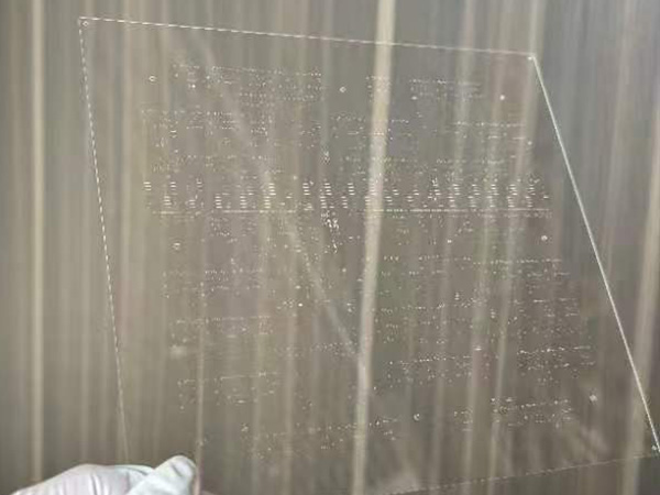
Glass substrates serve as a critical foundational material for liquid crystal panels and semiconductor packaging, characterized by high flatness, chemical stability, and dimensional precision
Glass Substrate Technology: Industry Applications, Material Characteristics, and Market Trends
1. Overview and Applications
Glass substrates serve as a critical foundational material for liquid crystal panels and semiconductor packaging, characterized by high flatness, chemical stability, and dimensional precision . They are primarily used in:
TFT-LCD/OLED display devices (e.g., smartphones, TVs, monitors)
High-performance computing (HPC) applications, including AI chips and high-bandwidth memory (HBM) manufacturing
In liquid crystal panels, glass substrates account for up to 20% of raw material costs, directly impacting key performance metrics such as resolution, light transmittance, and energy efficiency
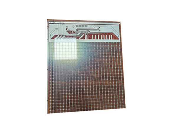
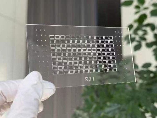
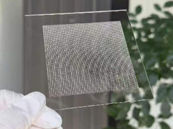
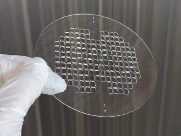
In semiconductor packaging, glass substrates replace organic substrates to address warpage issues. Their high wiring density enables 2.5D/3D integration and chiplet interconnection, achieving a 10× increase in interconnect density and a 30% reduction in power consumption
2. Market Dynamics and Production Trends
The world’s first semiconductor packaging glass substrate plant is expected to complete validation and begin mass production in Q4 2024 .
Global leaders like Intel and Samsung plan to mass-produce glass-based packaging solutions by 2026, while domestic manufacturers (e.g., BOE, Visionox, Rainbow Group, Dongxu Optoelectronics) are accelerating investments.
BOE’s 8.6-generation AMOLED production line (2290mm × 2620mm glass substrates) successfully lit its first product in December 2025, with a design capacity of 32,000 substrates/month and mass production expected in 2026 .
Samsung Electro-Mechanics and Sumitomo Chemical have signed a memorandum of understanding to establish a joint venture for glass core mass production, targeting semiconductor-grade glass substrates by 2027.
Process | Advantages | Limitations |
Float Process | Low cost, scalable production | Surface requires polishing, lower purity |
Overflow Fusion Process | Non-contact forming ensures ultra-clean surfaces | Dominates mainstream markets (>60%) |
Slot-Draw Process | Thickness precision up to ±0.01mm | Complex equipment, higher costs |
Photolithographic Etching | Precision finishing for AMOLED displays | High-resolution but resource-intensive |
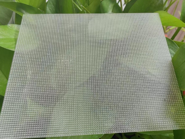
Glass substrates excel in:
· High Flatness & Surface Smoothness: Meets demands for sub-micron precision in chiplet integration.
· Superior Optical Properties: Ensures high light transmittance and uniformity for displays.
· Thermal Stability: Maintains structural integrity at temperatures exceeding 400°C.
· Chemical Inertness: Resists acid/alkali corrosion, ideal for harsh environments.
· Dimensional Stability: Minimizes thermal expansion (CTE ~3.5 × 10⁻⁶/K), ensuring reliability in multi-chip modules.
· Mechanical Strength: Flexural strength > 400 MPa, enhancing durability in high-stress applications.
Kartain specializes in advanced glass substrates tailored for AI chip packaging, AMOLED displays, and high-frequency 5G/6G components. Our strengths include:
· Precision Manufacturing: 5μm line width capability using mSAP 3.0 technology.
· Custom Material Formulation: Dielectric constant (Dk) as low as 3.8 @ 10GHz for ultra-low signal loss.
· Rapid Prototyping: Full validation in <7 days, with scalable mass production.
· Global Supply Chain: In-house glass synthesis ensures zero dependency on external suppliers.
Industry | Use Case | Kartain’s Value |
AI/HPC | Chiplet stacking (e.g., NVIDIA H100) | 30% higher interconnect density vs. organic substrates |
AMOLED Displays | High-precision substrates | 5μm photolithography ensures 8K resolution support |
5G/6G Infrastructure | mmWave antenna arrays | Dk=3.8 enables ≤0.15 dB loss @ 40GHz |
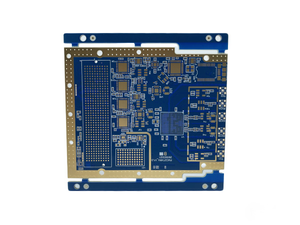
High Frequency PCBs are specialized printed circuit boards designed to handle and transmit high-frequency signals, typically operating above 1 GHz, with some applications extending into the millimeter-wave band (30 GHz and beyond). These boards are engineered to maintain signal integrity and reliability during high-speed data transmission, making them indispensable in modern high-speed communication and electronic syste
High Frequency PCBs are specialized printed circuit boards designed to handle and transmit high-frequency signals, typically operating above 1 GHz, with some applications extending into the millimeter-wave band (30 GHz and beyond). These boards are engineered to maintain signal integrity and reliability during high-speed data transmission, making them indispensable in modern high-speed communication and electronic systems.
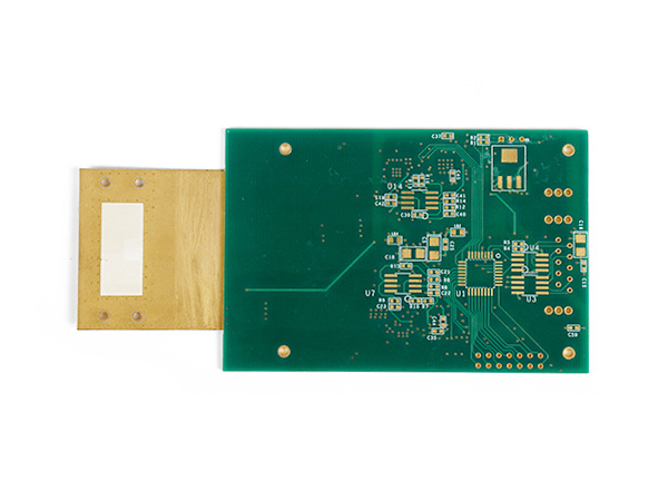
Product name: High frequency PCB
Material: Roger RO4350B + Shengyi S1000 FR4
Layers: 4layers
Copper: 1oz
Thickness: 1.20mm
Surface finishing: Immersion Gold 2U"
Soldermask: Taiyo Green soldermask
Application: communication device
Reach out to us via chat, phone, or our simple contact form.
Get a FREE Quote Today
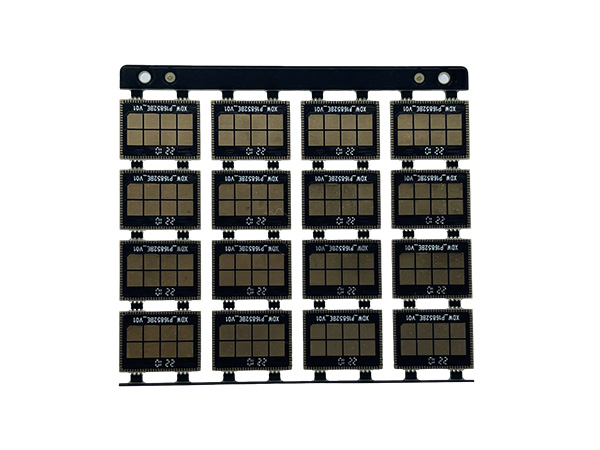
Our business scope includes IC substrate design and simulation, IC substrate manufacturing, IC packaging and testing, as well as comprehensive hardware assembly services(PCB & PCBA).