


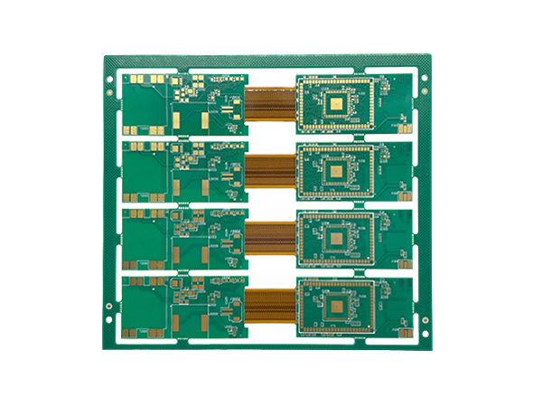
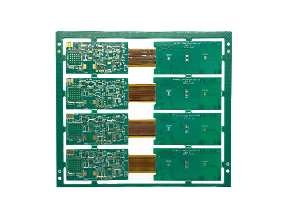
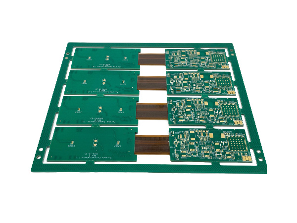
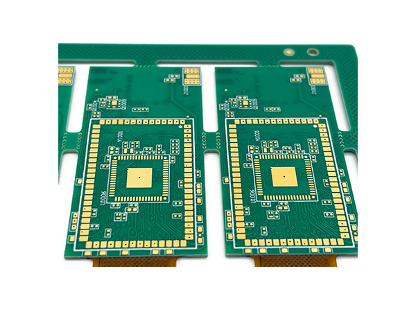
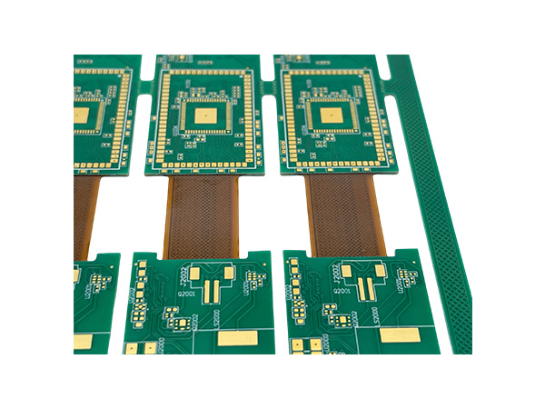
Name:communication devide flex rigid pcb Material: IT180 TG180 FR4 Thickness:1.60mm Layer:6L Copper:35um
Name: | Communication devide flex rigid pcb |
Material: | IT180 TG180 FR4 |
Thickness: | 1.60mm |
Layer: | 6L |
Copper: | 35um |
Soldermask: | Taiyo green soldermask |
Surface finished: | Immersion gold |
Min.Line width | 75um |
Min.Line spacing: | 75um |
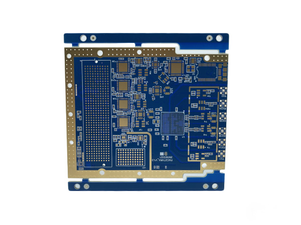
Kartain Technology CO.,LTD Medium and small batch multi-layer PCB board manufacturing, 4-32 layer PCB processing technology, minimum line width/spacing 2.5/2.5mil, copper thickness up to 12oz, meet the high heat dissipation requirements of power products,support blind hole, nickel palladium, selective gold, step hole groove, inner and outer layer impedance matching, resistance range: 45-110Ω.
Multilayer PCB boards production capacity:
1 | Layer | 1-32layer | |
3 | Raw Material | FR-4 | |
4 | Soldermask | Taiyo,Guangxin | |
5 | Max size | 1000×600mm | 4layer:1000*500mm |
6layer:900*500mm | |||
8layer:625*500mm | |||
10/12layer:400*300mm | |||
6 | Min size | 1×1mm | |
7 | Max boards thickness | 6.0mm | Standard:0.10/0.15/0.25/0.3/0.4/0.6/0.8/1.0/1.2/1.6/2.0/2.4/3.0mm |
8 | Min boards thickness | 0.10mm | |
9 | Min core thickness | 0.04mm | 40um |
10 | boards tolerance | ±10% | Min. 0.03mm |
12 | bow and twist | 0.75% | special controlled ≤0.5% |
13 | Max drilling | Φ6.5mm | Special > 6.5mm |
14 | Min drilling | Φ0.05mm | Standard: > 0.15mm |
17 | Min copper thickness | 1/8oz | standard: 1/2oz |
18 | Max copper thickness | 12oz | standard: 2-6oz |
23 | PTH tolerance | ±0.075mm | Special: ±0.05 |
24 | NPTH tolerance | ±0.05mm | |
25 | Hole shift tolerance | ±0.05mm | |
26 | Vias copper | ≥20μm | |
27 | Outlayer design rule(Line width/spacing) | T/Toz: 2.5mil/2.5mil(T=1/3oz) | |
H/Hoz: 2.5mil/2.5mil | |||
1/1oz: 3mil/3mil | |||
2/2oz: 6mil/6mil | |||
3/3oz: 10mil/10mil | |||
4/4oz:14 mil/14mil | |||
28 | Inner layer design rule (Line width/spacing) | T/Toz: 2.5mil/2.5mil(T=1/3oz) | |
H/Hoz: 2.5mil/2.5mil | |||
1/1oz: 3mil/3mil | |||
2/2oz: 6mil/6mil | |||
3/3oz: 10mil/10mil | |||
4/4oz:14 mil/14mil | |||
29 | Etching tolerance | ±20% | Special: 10% |
34 | Min soldermask bridge | 2mil | |
35 | Soldermask filled vias | ≤0.45mm | |
36 | electroless nickel immersion gold/nickel | 100-200uin(μ") | |
37 | ENEPIG standard | NI:200u" | |
Pd:1-10u" | |||
Au:1-10u" | |||
38 | electroless nickel immersion gold/gole | 1-3uin(μ") | special: 5-200U" |
39 | Tin thickness(HASL) | 2-40μm | |
40 | Selective Electric gold + Gold finger | AU:3-100u" | no plated line residual |
42 | Routing tolerance | ±5.2mil(0.13MM) | Larser ±2mil(0.05MM) |
43 | Hole to edge tolerance | ±7mil(0.177MM) | Special ±6mil(0.15MM) |
44 | Min inside Angle | R≥0.5mm |
Email us, we will send the multilayer PCB stack up PDF file to you for design reference.
High Frequency PCBs are specialized printed circuit boards designed to handle and transmit high-frequency signals, typically operating above 1 GHz, with some applications extending into the millimeter-wave band (30 GHz and beyond). These boards are engineered to maintain signal integrity and reliability during high-speed data transmission, making them indispensable in modern high-speed communication and electronic syste
High Frequency PCBs are specialized printed circuit boards designed to handle and transmit high-frequency signals, typically operating above 1 GHz, with some applications extending into the millimeter-wave band (30 GHz and beyond). These boards are engineered to maintain signal integrity and reliability during high-speed data transmission, making them indispensable in modern high-speed communication and electronic systems.
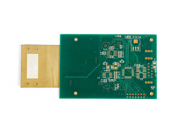
Product name: High frequency PCB
Material: Roger RO4350B + Shengyi S1000 FR4
Layers: 4layers
Copper: 1oz
Thickness: 1.20mm
Surface finishing: Immersion Gold 2U"
Soldermask: Taiyo Green soldermask
Application: communication device
Reach out to us via chat, phone, or our simple contact form.
Get a FREE Quote Today
Our business scope includes IC substrate design and simulation, IC substrate manufacturing, IC packaging and testing, as well as comprehensive hardware assembly services(PCB & PCBA).